| Warning | ||
|---|---|---|
| ||
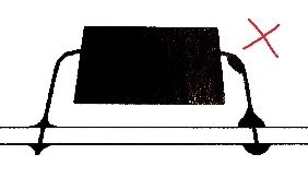
Use protective eyewear while soldering! Position the fume extractor close to- and over your working area! |
| Note |
|---|
High quality, fairly expensive soldering equipment is available at Omega Verksted. Please be careful with it, and ask a board member if you are unsure about something. |
See also: Soldering Equipment
Basics
- Do not use the soldering iron to exert physical force. Use pliers or other appropriate tools if you have to hold something in place or apply pressure.
- Use a soldering tip of appropriate size. If the solder joint is not heating up fast enough, usually the thing to do is to use a bigger soldering tip. A very coarse rule of thumb is that the soldering tip should be around the same size as the pad on your PCB. You can ask a board member if you can't find a bigger tip.
- The Metcal soldering stations at Omega Verksted do not allow for adjusting the tip temperature, because they automatically use the optimal tip temperature for the lead free solder stocked by Omega Verksted, about 412°C.
- There is a substance called flux that is a component of solder. Basically this serves to make the liquid solder flow correctly and distribute itself onto the component pins/pads. Flux is completely essential to soldering.
- Flux is single use, meaning that it will only function for a single heating. When initially soldering a joint, the flux in the solder thread will be sufficient. If you have to reheat a joint, additional flux must be added externally. At Omega Verksted, you can find additional flux in the Poison Fridge.
- When adding external flux, don't be afraid to add too much (although please don't waste excessively)
- There should be a small amount of tin on the soldering iron when it is in use, for any soldering operation. This will increase the contact surface area and improve thermal transmission.
- If there is oxide on the soldering iron (brownish-black stains), clean it off on the brass wool on the workstation while the iron is hot.
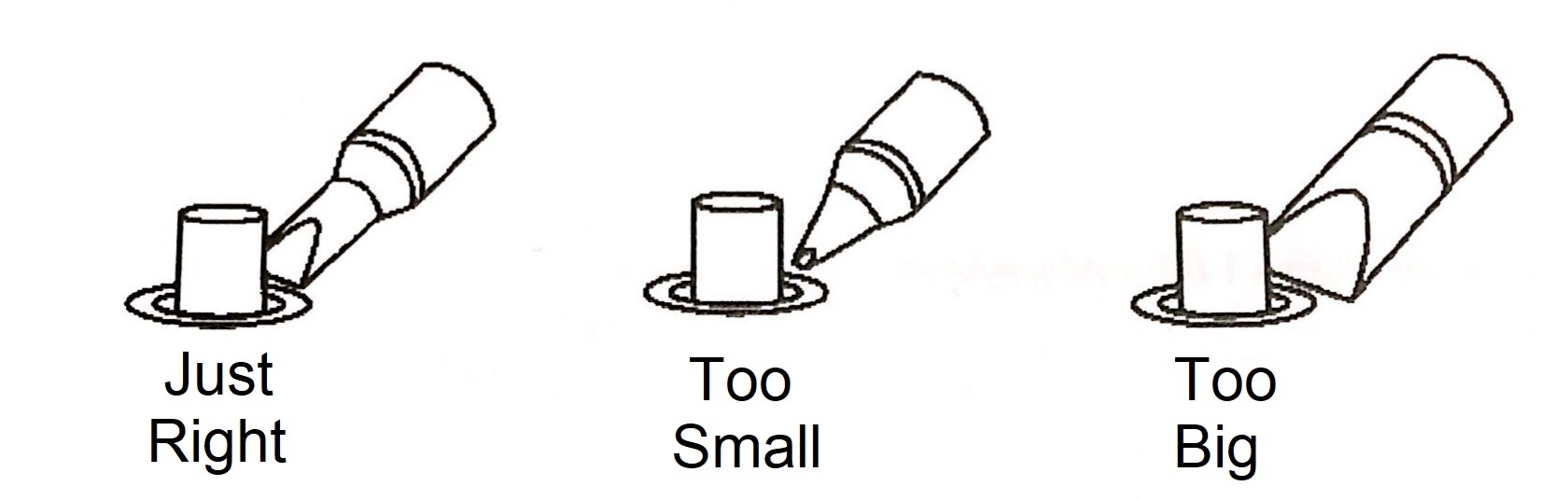
- In general, soldering a joint should take around 2-5 seconds.
- In general, the solder joint should have a "nice" slope. It should not be too concave or convex.
- Use a claw stand ("helping hand") to align the items you are soldering if necessary. Alternatively you can ask someone to help you hold something.
- Component legs should be cut before soldering.
- When finished, add some tin to the soldering iron. This will extend the lifetime of the equipment.
Desoldering
- When using a solder wick, you should add some flux to the solder joint you want to desolder.
Advanced
Although the following information could be useful for a beginner as well, you shouldn't be too concerned with it if you are just starting out. Soldering is the best way to learn soldering.
Types of Solder
There are a great many types of solder available, but at OV we usually try to adhere to lead free tin-silver solder alloys.
Leaded
- Sn60/Pb40
- A classic old-timer
- Easy to work with, fairly oxidation resistant
- Low Thermal Conductivity, can be held liquid for quite a while
- 188 °C
- Sn63/Pb37
- Eutectic
- Low TC
- 183 °C
Lead Free
- Sn93
- Sn95
Weird
- Bismuth-Tin Solders
- Indium-Tin Solders
- Indium-Bismuth Solders
- Pure Tin Solders
- Silver Solder
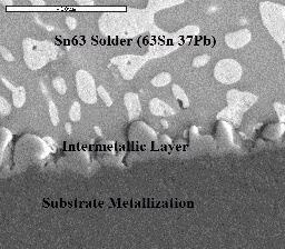
Intermetallic Layer
The goal of optimal soldering is to create an intermetallic layer (the layer of bronze between the copper and the tin) of the optimal thickness. This has been empirically determined to be around 1μm. For most applications, this will be achieved when the solder is heated to the correct temperature, the solder flows across the copper to cover all the areas of the joint ("wetting"), and the joint is heated for around 2-5 seconds. Heating the joint for too long will result in an intermetallic that is too thick.
- If the intermetallic is too thin, the joint will be mechanically weak.
- If the intermetallic is too thick, the joint will become brittle.
Over time, the intermetallic will passively become thicker on its own. This can contribute to the deterioration of old electronics.
Wetting
In soldering, wetting is the ability of the liquid solder to flow over and cover the desired surfaces of the components, wires and PCB pads. The degree of wetting (wettability) is determined by a force balance between adhesive and cohesive forces. Good wetting is achieved when the solder is heated to the correct temperature, there is sufficient active flux and the surfaces to be soldered are not contaminated with dirt, fat or oxides. Active flux will to a large degree remove impurities, but it doesn't have infinite capacity to clean.
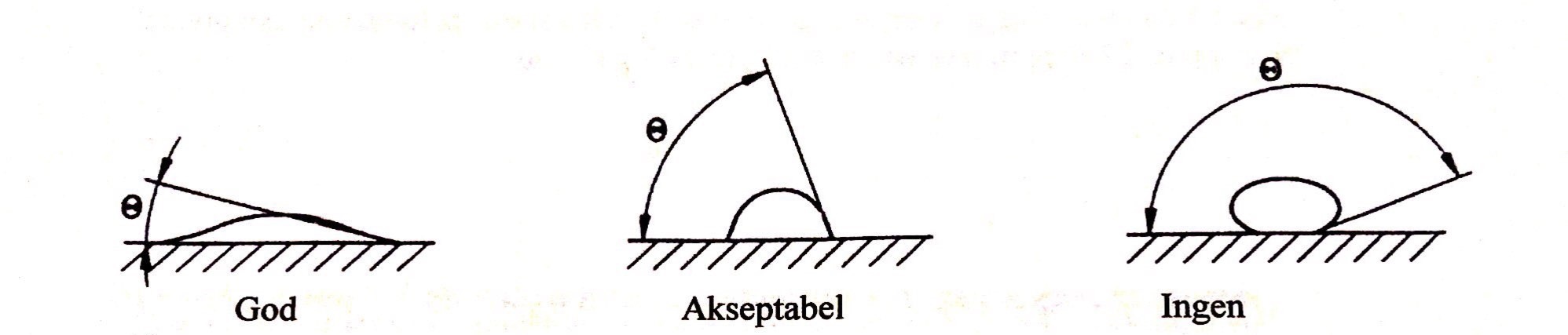
Wetting is usually measured by the contact angle of the joint:
- A very shallow angle means the liquid phase has such a strong affinity for the surface and so little resistance to flow it spreads evenly.
- A shallow angle
The distinguishing appearance of wetting may be confused with large excesses of solder, for small joints this may be hard to distinguish.
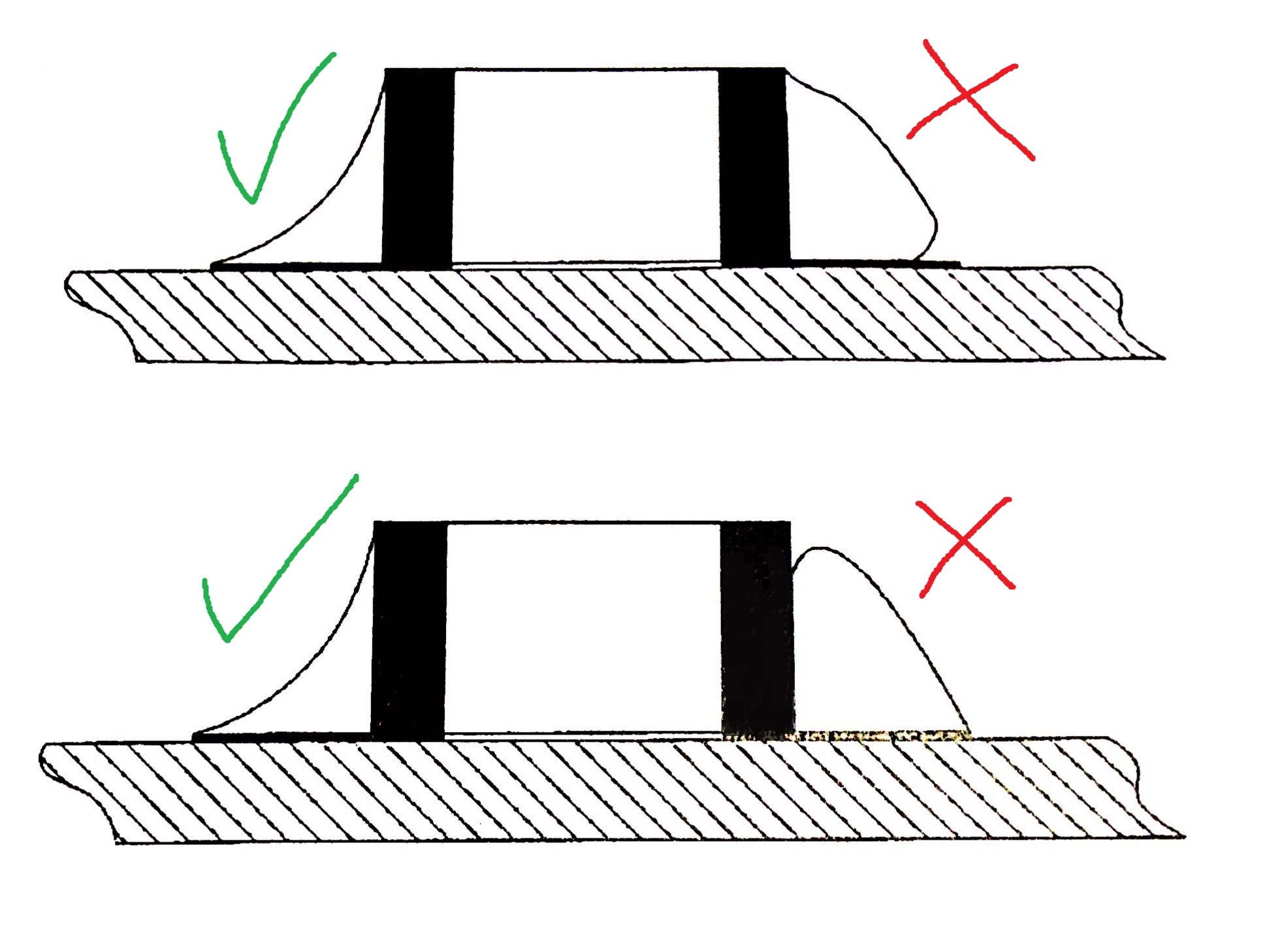
- A Concave joint indicates good wetting and a contact angle well below 90 degrees, and is easily visible.
- A Convex joint with excess solder may be a well wetted joint and can be partially identified by a good surface finish and good deformation around surfaces, but this is not a good measure. Excess solder is a poor practice and should be avoided, as inspection is made more insecure.
Flux
Flux (norwegian: Fluss) is a chemical cleaning agent, flowing agent, and/or purifying agent (Wikipedia article). One of the roles of flux is soldering is to prevent and remove copper oxides on components and PCBs. Tin based solder attaches very well to copper, but poorly to the various oxides of copper, which form quickly at soldering temperatures. By preventing the formation of metal oxides, flux enables the solder to adhere to the clean metal surface rather than forming beads, as it would on an oxidized surface. There are various types of flux:
- Resin based
- Synthetic
- Water based
After soldering is complete, there will often be some residue of burnt flux left. This may be cleaned, for example with Isopropyl-alcohol (some components may be damaged by this) or using an ultrasonic cleaner. If you are selling the electronics, or you want to make a good impression with it, you should clean it.
Left to right: Decreasing quality of wetting
Stress relief
Many components have stress relief "built in". In Through Hole components (TH), the legs serve this function. The same goes for IC packages with for instance "seagull" legs, such as QFP packages. No-lead packages such as QFN, do not have this advantage. Putting too much solder onto the leads of a component will negatively affect the stress relief ability, and should be avoided.
Temperature
With surface mounted components, it is generally recommended that the core of the component (generally the IC) should not experience a temperature rise of over 3°C per second.
The soldering temperature is the target temperature of the solder during soldering. It should be 60 - 90°C higher than the melting point of the solder. In turn the tip temperature should be 72-92°C higher than the soldering temperature.
Inspection
Various errors can be detected by closely inspecting the solder joint. A microscope will come in handy.
| Error | Severity | Description | Cause | Action |
|---|---|---|---|---|
| Cold soldering | Bad | Solder joint displays wrinkles, stripes or lines. Solder may be clearly separate from the component and/or the copper PCB. | Soldering temperature was too low. Usually thermal conduction is too poor (tip too small or not clean), or the joint was not heated for long enough. | Remove solder, clean and resolder. Make sure to solder for ~2-5 seconds with an appropriate tip. |
| Delamination | Catastrophic | PCB becomes deformed. Layers of the PCB may come apart. | PCB was overheated. Usually the joint/circuit was heated for too long. | (Irreparable) |
| Overheated joint | Poor | Solder has a finely grained, crystalline appearance. | Solder was overheated. Usually the joint/circuit was heated for too long, or there is a mismatch between the tip temperature and the solder used. | Remove solder, clean and resolder. Make sure to solder for ~2-5 seconds with an appropriate tip. |
| Porous solder | Poor | Solder joint has many small holes and/or grainy surface | Solder was overheated, combined with contamination. Usually the joint/circuit was heated for too long. | Remove solder, clean and resolder. Make sure to solder for ~2-5 seconds with an appropriate tip. |
| Icicles | Poor/Ok | Icicle-like structures or spikes | Solder was cooled down too fast. | Add plenty of flux and reheat for better wetting. |
| Solder bridges | Bad | Connections (short circuits) between pads or pins | Too much solder on the tip, often in combination with insufficient flux. | Remove solder bridges, add plenty of flux and reheat. |
| Dewetting | Bad | Solder has not flowed to all regions of the pad | Poor wetting, caused by contamination or insufficient flux. | Remove solder and clean. Preapply solder ("fortinn" loddestedet) before resoldering. Make sure to solder for ~2-5 seconds with an appropriate tip. |
| Dross | Bad | Charred areas on the surface of the solder | Contamination in solder, on components or on PCB. | Remove solder, clean and resolder. Make sure to solder for ~2-5 seconds with an appropriate tip. |
| Crack | Catastrophic | Cracks in the solder joint | Movement in the joint before solder has cooled. | Remove solder, clean and resolder. Make sure to solder for ~2-5 seconds with an appropriate tip. |
| Blobs | Bad | Blob around joint: Contact angle above 90 Degrees | Excessive solder has been applied. May if resoldered lead to a bridge, can also occlude joint making inspection of surface wetting impossible. | Remove solder, clean and resolder. Make sure to solder for ~2-5 seconds with an appropriate tip. |
Surface Mount- specific techniques (Advanced)
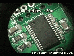
Reflow Soldering
The most common technique in industrial electronics manufacturing.
Instead of conventional solder wire, solder paste is used. Solder paste has the same ingredients as solder thread, but instead of being a solid wire, tiny beads of solder are suspended in a viscous flux, resulting in a gel-like substance. In addition to being solder, it also weakly glues the components to the PCB even before soldering.
Instead of using a soldering iron, the entire circuit is heated with a precise temperature profile (temperature as a function over time). Done correctly, reflow soldering generally gives better results for small or fine-pitch components unless you are extremely good at hand soldering. Either way, it also gives much better repeatability and process control, which are the main reasons it's the most common method in industrial manufacturing.
The components are free to move with the flow of the solder, and adhesive and cohesive forces (surface tension) will actually move the components towards the correct placement to some degree, although this effect has its limits. See gifs to the right.
Omega Verksted has facilities for doing reflow soldering, see Reflow Oven.
(Click for satisfying gifs)
|
|
|
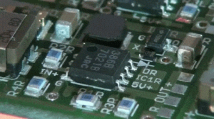
Different Package Types
Some packages with gull-wings like standard 50mil pitch SOIC packages have long, wide, well spaced pads and are extremely easy to solder and inspect, as they have well exposed pins with plenty of space for large pads.

Temperature Profile
The Soldering process has a number of steps, all with their important functions.
- Preheating:
Just heating up the board, making the flux flow and activate.
Fairly long, relatively fast temperature gradient - Soaking:
Heating the solder to just under melting, cleaning surfaces with active flux
Fairly long, shallow temperature gradient - Reflow ramp-up
Heating up components to somewhat over melting point
Short, high gradient - Reflow peak & hold
Letting solder balls immersed in flux coalesce, wet and bind nearby metallic surfaces
As short as possible, low gradient - Cooling
Constant gradient, slow enough to not cause major thermal gradients across the boards that can cause differential expansion stresses warping the board
As slow as practical

Types of Defects
Various errors can be detected by closely inspecting the solder joint. A microscope will come in handy.
| Error | Severity | Description | Cause | Action |
|---|---|---|---|---|
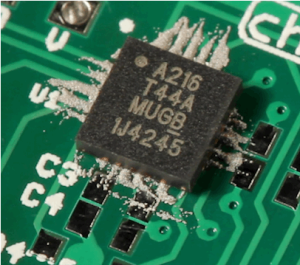
| Loose Solder Balls | Ok | Some solder paste has gone off a pad and drifted across the board. | Not a major issue if encapsulated by hard flux, but can be a shorting risk if balls are large. | Clean Board |
| Sintered Sponge Joint | BAD | Solder looks spongy and brittle, has almost no strength and looks like a rough sponge. Parts easily fall off and joint can be scraped off with a fingernail. | Far too long soak time, too high heat. All flux has burnt away before solder has melted, balls have stood stacked and oxidised before melting | Reduce profile time significantly, lower soaking heat. |
| Partially melted Balls on surface | Ok | The soldered joint seems mostly fine, but there's solder | The preface to the above sintered sponge, but not a direct issue. Marginal amounts of flux on outer balls, partial sintering has occured. | Reduce soak time |
| Oxidized surface | Poor | There is a strong, dull gray coating on all pads or a rainbow colored oxidation layer on exposed metal | Too high heat for too long, peak temperature is too high. Risk of burning board, delamination, frying chips | Lower soak and peak heat, reduce time |
| Unmelted paste | Poor | There is paste on the board that hasn't melted, there is still liquid flux in the paste | Too low heat, too short profile | Increase soak and peak temperature, profile time |
| Tombstoned Chips | Bad | Components have flipped vertical and stand on one pad, looks like a toombstone | Pads too wide or far apart, | Shrink footprint, use less solder paste, heat board more evenly |
| Head-In-Pillow | Bad | Upon closer inspection the solder has melted but not wetted the pad at all, the pad is just resting on top of the blob of solder | Too agressive heating causing one pad to heat up before the other and heat burning away enough flux that the affected pad has had more surface tension than it should | Adjust Profile to slower ramp, less soak time |
| Discolored Board | Ok | Copper surfaces, soldermask, chips and whatnot else are discolored, either darkened, brown | Way too high heat for far too long, peak temperature is too high. Risk of burning board, delamination, frying chips | Lower soak and peak heat, reduce time |
| Burnt Chips | Catastrophic | Many chips die near randomly across boards when tested. Probably comorbid with oxidised surfaces and board discoloration | Soldering profile is dangerous to part. Most IC's are surprisingly resilient and designed to be reflowed with lead-free processes at up to 270C for >30s, any oven will have to be maliciously or stupidly programmed for this to happen. Sentitive parts like sensors, precision voltage references or | Use recommended or tried and tested profile, not your own bizarre "it felt right"- profile. |
| Popcorning | Catastrophic | Chips may have cracks or holes in their casing, popping noises may be heard from outside the oven | Moisture has over time entered the chip, and rapid heating has caused the water to superheat to high pressure steam, cauing enough stress to crack the chip. Thin QFP's, DFN's, Large BGA's most affected. Rather uncommon for most parts and not a worry for single runs, however very significant in volume runs | Reduce parts' exposure to a humid atmosphere; use fresh components in dehumidified bags, bake parts before placement according to their MSL-rating, don't use old parts. |
| Oxidised pins | Bad | Part doesn't properly wet solder unless scraped or applied force to | Part has been exposed to air for too long, and tin coating on pin has corroded. Mostly a problem with grandpa's Ham radio replacement parts. | Electronic Parts have a shelf life, use new (not 10 year old and poorly stored) parts. |
Metallurgy, Advanced Inspection
Eutectic Alloys, Liquidus, Solidus and Glass Transition
Some packa
Material defects, failures over time
The metallurgy of soldering processes is somewhat complicated and unbearably dry, the open literature is usually poorly explained, case specific and
| Type | Description | Causes | Caused By |
|---|---|---|---|
| Cracks | Clean Board | ||
| Voids | |||
| Thick Intermetallic Layer | |||
| Short, stiff lead | |||
| Die CTE (Coefficient of Thermal Expansion) Mismatch | In Heating-Cooling cycles, large shear forces can occur | ||
Lead-Board CTE mismatch | |||
| Poor Homogeneity (multi-alloy solder) | |||