| Table of Contents |
|---|
Teori
Bakgrunn
TBD
Virkemåte
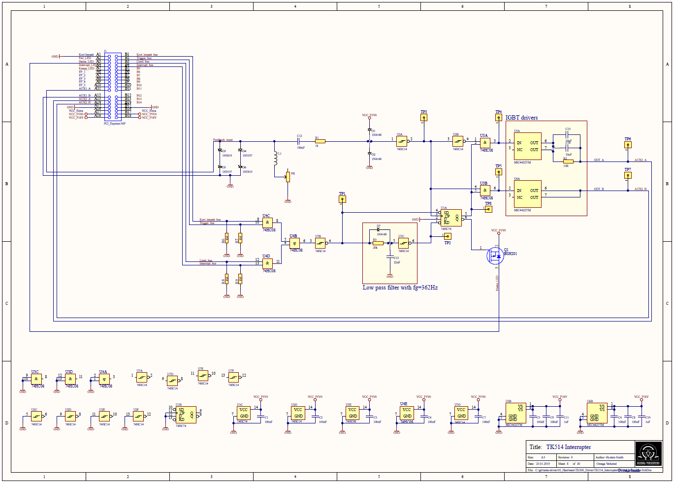
The interrupter generates the signal which drives the resonant circuit (coil rig) at its resonant frequency f0. As long as the input signal X2 is high the output produces a square wave with fundamental frequency f0. It does this by means of a positive feedback loop. The feedback signal X8 is retrieved with a sensing transformer around the output wire from the power amplifier (section 2.4), before being clamped, rectified, and schmidt triggered. This results in a cleaned up normalized representation of X8, lets call this signal X80. The flanks of X80 represents when the output current passes zero (this is when we want to switch the polarity of the output X5). X80 is fed to the output via gates controlled by a latch. X5_B is inverted in relation to X5_A (for push-pull operation). This circuit is shown in fig. 2.5, U1A is the latch witch is central to the operation of the interrupter. It has Four inputs SD, CP, D, and RD, wich are ’Set Data’ (active low), ’Clock Pulse’, ’Data’, and ’Reset Data’ (active low) respectively. And two outputs; Q wich is the normal output, and Q inverted wich is the inverted of Q at all times, Q inverted is unused in this circuit.
...
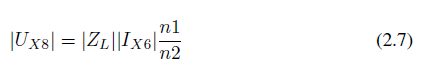
The relation between the peak voltage jUX8j over R2 and L1 is shown in eq. (2.7) assuming X8 is sinusiodal.
Reset network
The function of the network connected to the reset (RD) of the latch (U1A) is to reset the latch after a delay in the case that a zero crossing is not detected on X8 after X2 goes low. Note the inverting schmidth triggers U2C and U2D on both sides of the network. When X2 goes high the input of U2D goes low immediately due to the capacitor C2 being discharged through D7, but when X2 goes low the capacitor C2 will be charged through R3 and there will be a delay before the latch is reset. The time constant of R3 C2 is = 440 106s, the positive going threshold voltage of the inverting schmitt trigger (74HC14) is T+ = 2; 5V Wich is half of the supply voltage VCC_P5V0. We know that a capacitor is charged to 0; 5 VCC (where VCC is the applied voltage) after 0; 7 , thus the filter R3 C2 together with U2D introduces a delay of 0; 7 = 308s, or if we have a resonance frequency f0 of 110 kHz a delay of about 3,4 periods T = 1 f0 . If the synchronous shutdown does not work properly this filter should prevent or reduce noise from the interrupter not shutting down properly between each pulse on the input signal X2. This can also reduce the spark length if the spark is prevented from unintentionally continue longer than intended.
Input clamping and protection
D3-D6 are protection diodes which clamp the feedback signal to safe voltages. The network L1 and R2 introduces a tunable phase lead on the voltage. C1 and R1 is a filter to remove noise. D1 and D2 clamps the voltage to 0-5V.
IGBT Drivers
U5A and U6A are transistor drivers which amplify X4 and step up the voltage from 5V to 18V
External rescources:
| Widget Connector | ||
|---|---|---|
|
https://www.stevehv.4hv.org/new_driver.html
| Widget Connector | ||
|---|---|---|
|
Spec
Interruptindikator for alle slemme interrupts
Separat indikator for signalinterrupt
| View file | ||||
|---|---|---|---|---|
|
Versjoner
V0.0 (2009)
Changelog
- Laget av Dewald De Bruyn
Errata
- Ingen
V0.1 (2014)
Changelog
- Kokt fra 2009 design
Errata
- Ingen
V1.0
Release: 2017-03-16
Antall: 10
Changelog
- Bakplanifisert
- Lagt til testpunkter
- Lagt til (footprint for) potmeter og spole R4, L1 for å kunne justere phase lead
Errata
...
- Mangler thermals på jordpinner.
- C10 og C11 kan "krympes" til 0805
- C15 kan krympes til 0603
- D1, D2, D7 kan krympes til 0603Ingen
Produserte kort
| SN | V | Montert | Fungerer | Plassering | Kommentar | |||||||
|---|---|---|---|---|---|---|---|---|---|---|---|---|
| ? | 0.0 |
| 2009 Driver | |||||||||
| ? | 0.1 |
| 2014 Driver | |||||||||
| ? | 0.1 |
| Marintesla | |||||||||
| 01 | 1.0 |
| Den røde OLE-boksen |
Phase lead ikke justert, muligens ikke montert Jeg(Steinar) husker ikke hvorfor den ble tatt ut av driveren, så status er ukjent før den bir testet. | |
| 02 | 1.0 |
| TK500 SN:02 | ||||||||||||
| 03 | 1.0 | TK500 SN:01 | Ikke testet. Reworket av Erlend etter R1 falt av sammen med den ene paden. | |||||||||
| 04 | 1.0 | Øystein | Ikke testet | |||||||||
| 05 | 1.0 | |||||||||||
| 06 | 1.0 | |||||||||||
| 07 | 1.0 | |||||||||||
| 08 | 1.0 | |||||||||||
| 09 | 1.0 | |||||||||||
| 10 | 1.0 |