...
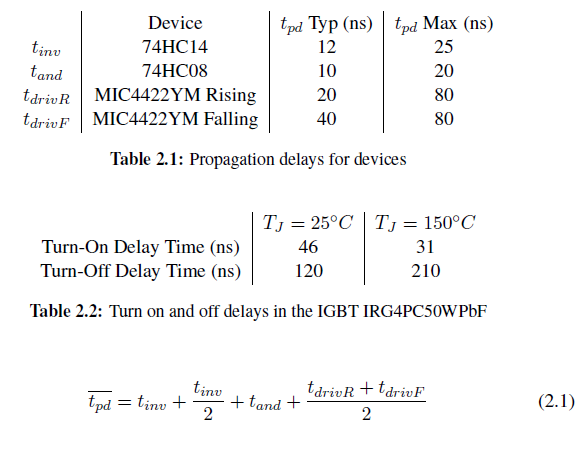
When X2 goes high the Set Data (SD) input of the latch U1A goes low and is activated, Reset Data RD goes high (inactive), and thus the output Q goes high. This enables the and gates U3A and U3B and allows X8’ to pass through, X4_B goes high and X4_A remains low, this causes a step response in the resonant circuit. The feedback transformer is oriented such that this current direction gives a negative voltage on X8 and thus still low signal on the input of U2A. When the current direction changes the signal on the input of U2A goes from low to high and X4_A goes high and X4_B goes low. This reverses the voltage on the resonant circuit in phase with the step response and triggers an additional step response in phase with the already ongoing one. This cycle continues untilX2 goes low. When X2 goes low SD goes low (inactive), but Q is still high until the next negative flank on X8 (inverted through U2A). When D (wich is strapped low) is clocked through the latch, Q goes low and both X4_A and X4_B goes low. And no further energy is supplied to the resonant circuit and the step response completes. In the case of the initial value of the output of U2A being low X4_A would go high first instead of X4_B and X8 would go high right away. Prompting X4_A and X4_B to invert immediately and switch the output while the current is not zero. Then the rest of the events happen as explained above. This immediate inverting of X4 may be unfortunate and a pull down resistor should be added at the input of U2A. The resulting signal on the output X7 is then Pulse Density Modulated (PDM). Phase Lead The function of L1 and R2 is to introduce a phase lead on the voltage of X8 in relation of the current on X8. The purpose of this is to compensate for propagation delays in the circuit and for switching delays in the transistors in the power amplifier (section 2.4). As the circuit is inductive, the voltage will lead the current. By adjusting the value of R2 the relation between the inductance and resistance is changed and thus the phase angle is changed. Thus the time between when the voltage crosses zero and the current crosses zero can be adjusted. This time should theoretically be equal to the time it takes the feedback signal X8 to propagate through the logic and for the transistors (IGBTs) in the power amplifier to turn on or off. So that we will switch when the current in the resonant circuit is zero (Zero current switching). This is to reduce energy lost from the resonant circuit and to minimize power burned in the transistors (when switching). From the datasheets we have the propagation delays tpd for the different devices in the propagation path shown in table 2.1. The there are two propagation paths one path contains one schmidt trigger (74HC14) more than the other, also the propagation delay in the mosfet drivers (MIC4422YM) differs for rising and falling outputs. The average propagation delay tpd from X8 on the input of U2A to X5 on the output of the mosfet drivers is then given by eq. (2.1) and results in tpd = 58 ns typical and 137,5 ns maximum.
In addition the delays from hysteresis in U2A th and switching delays in the transistors in the power amplifier tsw should be added to the desired phase lead td. Resulting in the desired phase lead td being given by eq. (2.2).
...