Teori
Bakgrunn
TBD
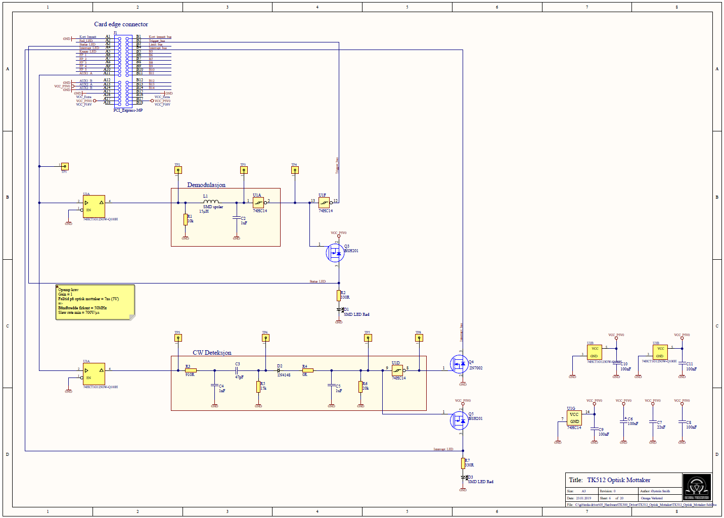
Virkemåte
The limiter prevents overcurrent in the coil rig by disabling the interrupter when
the peak current rises above a preset level. The limiter is shown in fig. 2.7
Figure 2.7: Limiter
The feedback signal is retrieved from the primary resonant circuit via the feedback
transformer L4. The diodes D1-D4 is a full bridge rectifier, schottky diodes are
used for low propagation delay. The rectifier is loaded with R2 and C3, R2 and C3
also functions as a noise filter with a cut off frequency fc given by eq. (2.8).
fc =
1
2R2C3
(2.8)
The cut off frequency fc decides how much noise is allowed through to the comparator
and thus how often the spark is shut down early unintentionally due to
noise. The spark being shut down unintentionally generates noise on the acoustic
signal.
The rectified signal is fed into a comparator, the other input of the comparator is
connected to a variable voltage controlled by a potentiometer. R3 is to set the
highest level the variable voltage can be set to. R4 is to pull the input of the
comparator low in the case that the potentiometer is disconnected.
The relation between the (peak) current in the primary resonance circuit and the
(peak) voltage on the input of the comparator is given by eq. (2.9).
2.3. Power Limiter 15
103 104 105 106 107 108
Frequency (Hz)
(2.9)
Where n1
n2
is the winding ratio of the feedback transformer, IX6 is the current
running in the primary resonance circuit, f is the fundamental frequency of IX6
(half the frequency of the signal on the input of the comparator because of the full
bridge rectifier). Given n1 = 1, n2 = 100, R2 = 10
, C3 = 1nF, f = 110kHz, we
get UX90
IX6
= 0; 1 Volts per Ampere.
If the voltage of X90 is higher than the voltage set by the potentiometer X10 the
output of the comparator goes low and resets the latch. The data input of the latch
is connected to VCC, on the next positive flank of the interrupt signal X2 the data
will be clocked to the output and the output will go high.
R5 is to give the possibility to tune the resistance of R2 by removing R2 from the
PCB and mounting R5 instead, R5 then replaces R2 in the calculations above.
R2 decides the range of current that can be sensed and compared to the preset
level. This is critical to the maximum amplitude attainable on the output and the
range of amplitudes attainable. And thus affects the volume and dynamic range of
the acoustic signal.
The output of the latch X3 is connected to the interrupter, as explained in section
2.2. A low signal stops the output of the interrupter. A high signal allows the
interrupt signal X2 to control the output.
Versjoner
V0.0 (2009)
Changelog
- Laget av Dewald De Bruyn
Errata
- Skjematikk eksisterer ikke
V0.1 (2014)
Changelog
- Delvis reverse engineret fra 2009, delvis eget design
- Splittet ut på eget kretskort
Errata
- Bærebølgedeteksjon fungerer ikke
- Inverterbufferet dør fra tid til annen
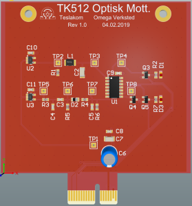
V1.0
Changelog
- Bakplanifisert
- Flyttet optisk plugg til eget kort
- Lagt til buffere før filterne
- Lagt til testpunkter
Errata
- Bærebølgedeteksjon fungerer ikke
Produserte kort
| SN | V | Visuell sjekk | Demodulator | Bærebølgedeteksjon | Interrupt LED | Status LED | Kommentar | |||||
|---|---|---|---|---|---|---|---|---|---|---|---|---|
| 1 | 1.0 | Hacket til delvis bærebølgedeteksjon | ||||||||||
| 2 | 1.0 | |||||||||||